Tuesday, December 20, 2011

ELECTRICITY FROM SUNLIGHT

PHOTOELECTRIC DEVICES

There are several types of devices commonly found in electronics that utilize the photoelectric effect. Some materials such as sodium or potassium have the ability to emit electrons when exposed to light. This property is called PHOTOEMISSION and is the basis for the phototube.

A second device utilizes the property of PHOTOCONDUCTIVITY and exhibits a change in resistance when exposed to light and is typically made from cadmium sulfide. Others include the phototransistor, photodiode and photo SCR.

SOLAR CELLS

The most important device, especially in today’s green movement, is called the solar cell.  A device typically made out of selenium or more likely silicon. The solar cell is considered a PHOTOVOLTAIC device and generates a voltage when exposed to light.

A solar cell starts out as an extremely pure silicon crystal that has been doped with a small amount (about 1ppm) of either Arsenic or Boron.

In a crystal of pure silicon, each silicon atom has four valence electrons and is bonded to four other silicon atoms by a shared pair of electrons (covalent bond).

Arsenic atoms have five valence electrons, four which are bound to the silicon atom. The fifth electron is fairly free to move around and this material is considered a “N” or donor type semiconductor.

Boron atoms have three valence electrons. These three electrons also bond to nearby silicon atoms. However, this leaves a shortage of one electron, leaving a positive hole in the crystal. This material is considered a “P” or acceptor type semiconductor.

When these two types of crystals (“N” type and “P” type) are joined, electrons tend to flow from “N” type (donor) to the “P” type (acceptor). However, the holes near the junction are quickly filled and the current flow ceases.

When sunlight strikes the cell, more electrons are dislodged. This creates more mobile electrons and more positive holes. Some of the free electrons and holes are produced within the depletion region (an area devoid of majority carriers) while others are generated outside of the region but also are drawn into it.

The free electrons in the region are swept from the P-type to the N-type material and the holes are drawn in the opposite direction. This produces a small voltage across the PN junction and if a load resistance is connected, a small current will flow through the load. This current flows from the N-type material through the load and back to the P-type material.

In the typical construction of a solar cell, the “N” type silicon layer is applied to a metal backplate which becomes the negative output connection. The “P” type semiconductor is diffused into the exposed face of the “N” type layer. This is known as a P-on-N device. An ohmic contact is then formed on the “P” type layer becoming the positive terminal.

These cells are also available in an N-on-P configuration. The main difference between the two configurations is that the active area of the P-on-N device becomes positively charged when exposed to light. For the N-on-P device, the active area becomes negatively charged. Also, the N-on-P cell has a lower dark reverse leakage than the P-on-N cell.

Since the output from a single solar cell is fairly small, only about 0.4VDC, multiple cells are usually connected in various series and parallel combinations to increase both the voltage and current to useful levels.

PURE CRYSTAL OF SILICON


SILICON DOPED WITH ARSENIC HAS EXTRA ELECTRONS


SILICON DOPED WITH BORON HAS POSITIVE HOLES


ELECTRON FLOW FROM DONOR TO ACCEPTOR


REFERENCE

Hill, John; Kolb, Doris. "Chemistry for Changing Times" Ninth Edition, 2001 Prentice-Hall

Wednesday, December 7, 2011

TC74 DIGITAL TEMPERATURE SENSOR

The TC74 is a digital temperature sensor that outputs an eight bit word that corresponds to temperature. The output is compatible with the IIC serial data bus interface. Temperature accuracy is +/- 2 °C from +25 °C to +85 °C and +/- 3 °C from 0 °C to +125 °C with a resolution of 1 °C. Package options are either TO-220 or SOT-23.

All TC74 sensors can be used with a supply voltage from 2.7 VDC to 5.5 VDC. However, the TC74 is available with specific supply voltages of either 3.3 VDC or 5.0 VDC. By matching the sensor to the supply voltage, better accuracy can be obtained. Also, each voltage can be obtained with eight different address values, allowing more than one sensor on a single IIC bus.

The eight bit output is in two’s complement form. Using the two’s complement number system allows a way to express both positive and negative numbers. In two’s complement, all numbers that have a most significant bit (MSB) of 0 are positive and all numbers with a MSB of 1 are negative. Therefore, the largest positive number that can be expressed as an eight bit number is 127/D or (01111111). Negative numbers consist of values from -1 to -128 with 0 being considered a positive number.

Some Examples:

+127 °C  =  0111 1111b
  +25 °C  =  0001 1001b
    +0 °C  =  0000 0000b
     -1 °C  =  1111 1111b
   -25 °C  =  1110 0111b
   -55 °C  =  1100 1001b

In order to display the correct negative value, I convert any negative numbers back into its positive number. I do this by taking the two’s complement of the negative number. Two’s complement = one’s complement + 1. The one’s complement is performed by inverting all bits, 1’s become 0’s and 0’s become 1’s.

EXAMPLE:

-1 °C   = 1111 1111 = 0000 0000 + 1 = 1
-25 °C = 1110 0111 = 0001 1000 + 1 = 25
-55 °C = 1100 1001 = 0011 0110 + 1 = 55
TC74 SERIAL PORT OPERATION

START Condition (S)
The TC74 continuously monitors the SDA and SCLK lines for a START condition (a high-to-low transition of SDA while SCLK is high) and will not respond until this condition is met.

Address Byte
Immediately following the START condition, the master must transmit the address byte to the TC74. The 7-bit address transmitted in the serial bit stream must match for the TC74 to respond with an Acknowledge (indicating the TC74 is on the bus and ready to accept data). The 8-bit in the address byte is a Read/Write bit. This bit is a ‘1’ for a read operation or ‘0’ for a write operation.

Acknowledge (ACK)
Acknowledge (ACK) provides a positive handshake between the master and the TC74. The master releases SDA after transmitting 8 bits. The master then generates a ninth clock cycle to allow the TC74 to pull the SDA line low. This action acknowledges that the TC74 successfully received the previous 8 bits of data or address.

Data Byte
After a successful acknowledge (ACK) of the address byte, the master must transmit the data byte to be written, or clock-in the data to be read. An acknowledge (ACK) will be generated after a successful write of a data byte into the TC74.

STOP Condition (P)
Communications must be terminated by a STOP condition (a low-to-high transition of SDA while SCLK is high). The STOP condition must be communicated by the master to the TC74.

The following is a C function that is used to send and receive data from the TC74.
It was written for the FREESCALE MC9S08 series 8 bit microcontrollers.

IIC REGISTER BIT DEFINITIONS

IICC:    IIC Control Register
IICD:    IIC Data I/O Register

IICC_TX:         Transmit Mode Select: 0 = Receive, 1 = Transmit
IICC_TXAK:    Transmit Acknowledge Enable
IICS_IICIF:      IIC Interrupt Flag
IICC_RSTA:     Repeat Start
IICC_MST:       Master Mode Select
IICC_RXAK:    Receive Acknowledge


IIC TC74 TEMPERATURE SENSOR DATA FUNCTION
void iic_tmpdata(void)

{
//GET TEMPERATURE DATA FROM SENSOR
//WRITE - SEND START BYTE
IICC_TX = 1;
IICC_TXAK = 0;
IICC = 0xB0;
IICD = 0x96;
while (!IICS_IICIF);
IICS_IICIF = 1;
while (IICS_RXAK);

//WRITE - SEND COMMAND BYTE
IICD = 0x01;
while (!IICS_IICIF);
IICS_IICIF = 1;
while (IICS_RXAK);

//WRITE - SEND CONFIGURATION BYTE
//$00 = normal mode, $80 = standby mode
IICD = 0x00;
while (!IICS_IICIF);
IICS_IICIF = 1;
while (IICS_RXAK);

//WRITE - STOP AND DELAY BEFORE READ
IICC_MST = 0;
iic_wait (50);

//READ - SEND SLAVE ADDRESS
IICC = 0xB0;
IICD = 0x96;
while (!IICS_IICIF);
IICS_IICIF = 1;
while (IICS_RXAK);

//READ - SEND COMMAND BYTE (TEMPERATURE)
IICD = 0x00;
while (!IICS_IICIF);
IICS_IICIF = 1;
while (IICS_RXAK);

//READ - REPEAT START COMMAND
IICC_RSTA = 1;
IICD = 0x97;
while (!IICS_IICIF);
IICS_IICIF = 1;
while (IICS_RXAK);

//READ - PERFORM DUMMY READ
IICC_TX = 0;
IICC_TXAK = 1;
TC74_data = IICD;
while (!IICS_IICIF);
IICS_IICIF = 1;

//READ - STOP
IICC_MST = 0;
iic_wait (50);

//READ TEMPERATURE
TC74_data = IICD;
}

CIRCUIT BOARD

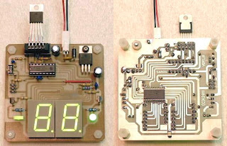
A relatively simple circuit board was designed to display the temperature data from the TC74 sensor. The microcontroller was a FREESCALE MC9S08QG8 operating at 3.3 VDC. Two LTS3401 (“0.8”) common anode green LED displays were used along with a CAT4016 constant current LED driver to drive the display segments.

The CAT4016 can drive up to 16 LEDS, making it perfect for two seven segment displays along with a decimal point on each display. Current limiting for the LED’s requires only a single 4K resistor. A 4K resistor will set the LED current at 15 mA per segment. The displays are directly driven and not multiplexed. I prefer direct drive as it lowers CPU overhead and power supply bus noise.

For a negative sign, I usually prefer to use the middle (“g”) segment on an LED display. Unfortunately, doing so in this case, with only two digits available,  would limit the minimum temperature display to only -9 °C. I decided instead to use a 2mm x 7mm rectangular green LED just to the left of the tens display as a negative indicator. This allows the minimum display to be -99 °C. The negative LED was controlled by an available port pin on the MCU.

The TC74 was connected to the PCB using a 2x5 pin connector made by 3M.
This would allow using a four conductor cable to connect the sensor for remote operation.


The single sided PCB measures 3in x 3in and was homemade using a photo negative process.

TC74 PCB SCHEMATIC

CLICK ON FOR LARGER IMAGE


TC74 PCB LAYOUT
TC74 PCB LAYOUT PDF


CLICK ON FOR LARGER IMAGE


FINISHED PCB


CLICK ON FOR LARGER IMAGE
 

TEMPERATURE DISPLAY ROUTINE

The display loop routine shows the temperature in both °C and °F. The example below indicates a temperature of  -10 °C and 14 °F. The program also includes a display test that lights all the display segments and the two indicator LED's when the PCB is powered up.

An alternate program could be easily created that stores the highest maximum temperature and also the lowest minimum temperature. The PCB has a PB switch which could control an interrupt (flag) that causes the display loop to display the high / low temperature as “HI” / (temp) and “Lo” / (temp) in both °C and °F. This is something I have done with a similar TC74 design that uses an LCD display.


CLICK ON FOR LARGER IMAGE

REFERENCE: MICROCHIP TC74 DATASHEET  http://www.microchip.com/