Monday, September 26, 2011

TC1047 TEMPERATURE TO VOLTAGE CONVERTER


The TC1047 is a linear voltage output temperature sensor. The output voltage is directly proportional to the measured temperature with an output voltage response of 10mV / °C

The output voltage range for these devices is typically 100mV at -40°C, 500mV at 0°C, 750mV at +25°C, and 1.75V at +125°C.

The temperature range is from -40 °C to +125 °C.
The accuracy is +/- 2 °C at 25 °C.

TEMPERATURE CIRCUIT OPERATION

In order to achieve the greatest accuracy, an output scaling circuit is used to convert the 100mV to 1.75V sensor output to 0V to +5V for use by the microcontroller’s analog to digital converter.

The 0V output is created by the “zero adjustment” pot which is set for -100mV (offset) and is summed with the output from the temperature sensor. This is performed by operational amplifier #1. The output from this stage is a negative voltage.

The total voltage output from the sensor is 1.65VDC (1.75V – 0.1V). This voltage needs to be amplified in a linear manner to a voltage of +5VDC. OpAmp #2 is used amplify the input by a gain of 3.03 (5.0V / 1.65V). Since the input from OpAmp #1 is a negative voltage, OpAmp #2 is configured as an inverting amplifier which will invert and amplify the negative input into a positive linear output from 0v to +5V. (set with the GAIN adjustment). A 2K resistor and a 1.0uF capacitor are used to filter the final output. A IN4148 diode protects the MCU input from any negative voltages should there be a circuit failure.

The negative five volts is created by a IC7660 voltage converter. The IC7660 will perform voltage conversions from positive to negative for an input range of +1.5V to +10V. Only two external capacitors are required to operate the internal charge pump and output filter.

The LM385 is a micropower voltage reference diode and is used to regulate the -5V output from the IC7660 to -2.0VDC.

MCU OPERATION

A FREESCALE MC9S08QD4 is used as an analog to digital converter and is also programmed to provide a “bit-banged” SPI output to control the FREESCALE
MC14489 five digit display driver. The MC14489 can be programmed to display a limited number of characters such as “°C” and a negative sign for temperatures below zero and also leading zero blanking. The green LED displays used are 0.8” high and are made by LITE-ON.


TEMPERATURE SENSOR CIRCUIT
 
CLICK ON FOR LARGER IMAGE


PROTOTYPE


TEMPERATURE CIRCUIT

Thursday, September 22, 2011

WIRELESS POWER

This project is a simple way of demonstrating inductive coupling. Many charging mats made for use with cell phones and other small electronics use a similar principle.

What we essentially have is an air core transformer. A convential transformer has iron laminations that efficiently couple the magnetic field between the primary winding and the secondary winding. However, in this case the lack of an iron core means that we must tune both the transmit and receive coils to resonate in order to create adequate power transfer.

The transmitter circuit is a simple MOSFET multivibrator. The charge – discharge cycle of the two 300pF capacitors causes the two MOSFET’s to alternately turn on and off. Normally a current limiting resistor is used between V+ and the MOSFET drain. In this application the resistor is replaced with one of the coil windings on each side of the center tap. The center tap is connected in series with a 10 ohm resistor and a 1 amp PTC fuse to the power source. The resistor and PTC fuse prevent excessive current flow should one of the MOSFETs fail. The 400pF capacitor and 10M resistor help with oscillator start-up when power is applied.

The receiver is simply a coil with a capacitor and an LED connected in parallel.
Most efficient coupling seems to occur when both coils are parallel with one another on the same vertical axis. With a supply voltage of 18 VDC, the LED would begin to light when held about 7 inches above the transmit coil. Coupling also occurs when the two coils are placed side by side on the same plane as shown in the photograph. The circuit will work with a supply voltage down to 4 VDC, with a corresponding decrease in coupling distance. A supply voltage of 10 VDC or greater seems to work best.

My prototype with a supply voltage of 12 VDC and a horizontal (plane) center to center distance between receiver coil and transmitter coil of 3 inches, I measured a receiver output of 8 VAC peak to peak at a frequency of 4.76 Mhz.

It was interesting to note that I got the same results with the coils stacked vertically on center also at a distance of three inches. At a distance of one inch vertically, the output was 10 VAC peak to peak with a slight increase in frequency to 4.8 Mhz.
The probe used was rated at 100 Mhz, 13pF and 10 meg and may have some loading effect on the results.

It is quite possible that there are modifications to this circuit that will make it work more efficiently. One thing to try is a transmit coil made with 18 or 16 ga wire and also with a different number of turns. Maybe two or four turns instead of ten or a larger diameter.

Also, you can experiment further by using four Schottky diodes in a bridge configuration with a filter capacitor to create a DC source to power a MCU or other electronics.


TRANSMITTER AND RECEIVER IN OPERATION


RECEIVER OUTPUT


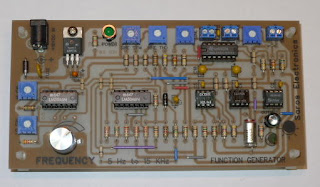
FUNCTION GENERATOR


This function generator features a tuning range of 5 Hz to 15 KHz and has SINE, SQUARE and TRIANGLE outputs. The circuit is based on a 555 timer operating as a Schmitt trigger. A CA3140 is used as a voltage follower to “read” the voltage across the timing capacitor. The CA3140 also drives the 555 and provides the triangle output. The triangle waveform is created from the charge and discharge of the timing capacitor from the constant current provided by a CA3080 operational transconductance amplifier (OTA). The square wave output comes directly from pin 3 (output) of the 555 timer.

The frequency is adjusted by a 1k pot along with a LM3046 transistor array used as an adjustable current source feeding the OTA. There is also a “HI CALpot and a “LOW CAL” pot to set the upper and lower frequency limits.

The SINE output uses another LM3046 that functions as a triangle to sine wave converter. There are also two trim pots that are used together to null the output distortion to 0.3% of less.

Both the TRIANGLE and SINE outputs are buffered by an LM3900 with the output adjustable from approximately 5V to 15V.

Finally, an LED is connected to the SQUARE wave output to provide a visual indicator.

The PCB measures 3.0in by 6.0in and made of 0.032in glass epoxy.

I know that there are single chip function generator IC’s available that does essentially the same thing as this. However, this design was more challenging and is easier to customize for a specific application.

Additional information about this design can be obtained from “THE IC TIMER COOKBOOK” by Walter Jung. Published in 1977 by Sams Publications.


                                    PCB ASSEMBLY


                                    PCB LAYOUT


                                   10KHZ SINE OUTPUT


                                   1KHZ TRIANGLE OUTPUT


Wednesday, September 21, 2011

1 AMP POWER SUPPLY

This is a variable voltage analog power supply based on the LM317 voltage regulator.

The voltage is adjustable from 1.2 VDC to 30 VDC via a “VOLTS ADJ” potentiometer. There is also a “MAX ADJ” trim potentiometer that can be used to limit the maximum output voltage. The input is protected by an auto-reset fuse. Input voltage can be either 6-24 VAC or 8-35 VDC.

AC inputs are rectified by four 1N5402 (3 amp) diodes in a full bridge configuration and filtered by two 2200uF electrolytic capacitors. The main output regulator is fan cooled allowing continuous operation at high current levels and high ambient conditions. The regulator has built-in thermal protection and current limiting. The maximum output voltage is 30 VDC (with an input of 24 VAC or 35 VDC) and the maximum output load current is 1.0 Amps DC at any voltage.

The PCB measures 3.0in by 4.5in and made of 0.032in glass epoxy.
 

                                    PCB ASSEMBLY


                                    PCB LAYOUT